What a GPU-Hour Actually Is
What is inside the thing called a GPU, the handful of numbers that describe it, why the number on every vendor slide is the least useful one, and who actually has to be involved before a chip becomes something you can rent
A GPU-hour is one hour of access to one graphics processing unit. That sentence is true and almost useless, in the way that "a barrel of crude is 42 gallons of oil" is true and almost useless. Nobody who trades crude thinks of it as 42 gallons. They think about sulfur, gravity, where the barrel sits, and which refinery wants it. Compute is heading the same way, and this series is about the physical facts that make the market price the way it does.
This first piece covers the unit itself: what is inside the thing called a GPU, the handful of numbers that describe it, why the number on every vendor slide is the least useful one, and who actually has to be involved before a chip becomes something you can rent.
Three things to know before anything else
Capacity moves in nodes, not chips. A node is one server holding eight GPUs wired together. You can rent a single GPU from a marketplace, but institutional capacity is delivered as nodes, racks and clusters, and even when the price is quoted per GPU-hour the surrounding configuration is part of what is being priced. The wiring is part of the product.
It is not storable. An idle GPU-second is gone the moment it passes. There is no inventory, no cost of carry, and no cash-and-carry arbitrage to anchor a forward curve. Anyone arriving from oil or grain should hold this at the front of their mind, because it is the single biggest structural difference, and it is why compute behaves more like electricity than like a barrel.1
It is not a single number. A GPU-hour has at least five independent specifications, and different buyers weight them differently. That is why no conversion ratio between chip generations exists, and why both exchange groups that have filed compute futures, CME with Silicon Data and ICE with Ornn, specified one contract per chip generation rather than a single "GPU" contract.2,3 Part 5 of this series makes that argument in full.
Vocabulary, briefly
A GPU is a processor that does enormous numbers of simple arithmetic operations at the same time. It was built to color pixels for video games. Neural networks happen to need exactly that kind of arithmetic, which is why a gaming chip became the unit of AI compute.
A model is a neural network: billions of numbers, called weights or parameters, learned during training. Running the model means doing arithmetic on those numbers. A "70B model" has 70 billion of them.
A token is the unit of text a model reads and writes, roughly three-quarters of a word. A model produces its answer one token at a time, and each token requires a pass through all the weights.
Memory, in this series, means the GPU's own on-board memory, called HBM (high bandwidth memory): stacks of memory chips sitting next to the processor. The model's weights have to be loaded into HBM before the GPU can use them.
Precision is how many bits the GPU spends storing each number. Fewer bits means each number takes less space and moves faster, at some cost in accuracy. The formats are named by bit count: FP32, BF16, FP8, FP4. The one fact you need for now is that at 8-bit precision each parameter takes one byte, so a 70B model occupies 70 GB.
Bandwidth is how many bytes per second can move from memory into the compute units. Capacity is the size of the tank; bandwidth is the width of the pipe.
Batching is processing many users' requests in one pass through the model instead of one at a time. It is the biggest single lever in the economics, and Part 2 explains why.
The factory
One picture carries most of this series. A GPU is a factory.
| GPU concept | Think of it as |
|---|---|
| Compute (TFLOPS) | How many machines are on the floor |
| HBM capacity | How big the warehouse is |
| HBM bandwidth | How wide the loading dock is |
| NVLink, the GPU-to-GPU link | How fast workers pass material between machines |
| Scale-up domain | How many machines are in the same room |
| Scale-out network | The roads between separate buildings |
| Power | How much utility service the factory can draw |
| Cooling | How much waste heat it can get rid of |
| Throughput | How much finished product actually leaves the building |
A factory with enormous machinery and a narrow loading dock produces very little. That is the whole memory-bandwidth story in one sentence, and it is why the loading dock, not the machinery, is usually the number that prices.
The five numbers
Every accelerator can be described with five quantities. The first four belong to the hardware; the fifth is what it costs to keep the hardware alive.
- Compute, measured in TFLOPS (trillions of floating-point operations per second). Raw arithmetic. Always quoted at a specific precision, and always the headline on the slide. Compute sets the ceiling. It rarely tells you what you will get.
- Memory capacity, in gigabytes of HBM. What fits on one GPU. If the model does not fit, it has to be split across several, and every split costs communication time on every operation.
- Memory bandwidth, in terabytes per second. The feed rate. A warehouse can be huge with one narrow dock, or modest with an enormous one, and those are different economic attributes. For the phase of serving a language model where it writes its answer word by word, bandwidth, not compute, is usually the limiting resource. Training and prompt- reading behave differently, and Part 2 separates them.
- Interconnect and domain size. How fast GPUs can talk to each other, and how many sit inside the fast domain: eight in a standard node, 72 in NVIDIA's rack-scale NVL72 systems.4 Part 3 is entirely about this number. For any model that spans more than one GPU, it decides whether the other GPUs can be used at all.
- Power. Watts per GPU and kilowatts per rack. This is the number hardware write-ups usually leave out, and it belongs alongside the other four, because the economic product is not a naked chip. It is an energized chip in a functioning building. A GPU that draws 1,400 W in a 130 kW rack does not exist commercially in a building wired for 40 kW racks, however good its other four numbers are.5
What the five produce is throughput: tokens per second, training steps per hour. That is what customers pay for.
Why the headline number fails
Compute is the least useful of the five, for two reasons. The first is that it is rarely the bottleneck. The second is that the number itself is unreliable until you ask three questions.
At what precision? FP4 figures are roughly twice FP8 figures, which are roughly twice FP16. Normalize before comparing.
Dense or sparse? Sparse figures assume half the weights are zero and can be skipped. The feature is real; the condition is rarely met. Ask for the dense number. NVIDIA's own product pages list the sparse figure with a footnote, so it is easy to grab the wrong one.6 Tensor core or general? The headline is matrix-multiply throughput on the specialized matrix units. Everything else runs far slower.
Here is the trap with numbers in it. Chip A claims 20 petaflops. Chip B claims 40. B looks twice as fast. But if A is dense FP8 and B is sparse FP4, strip the sparsity to get 20 dense FP4, halve it to convert to FP8, and B is at 10 petaflops. A is actually twice as fast.
The teaching trade: H100 versus H200
The H200 has identical compute to the H100. Same chip, same 1,979 dense FP8 TFLOPS. NVIDIA changed only the memory: 141 GB at 4.8 TB/s instead of 80 GB at 3.35 TB/s. The result, by NVIDIA's own benchmark, is up to 1.9 times the inference throughput on a 70B-parameter model.6,7
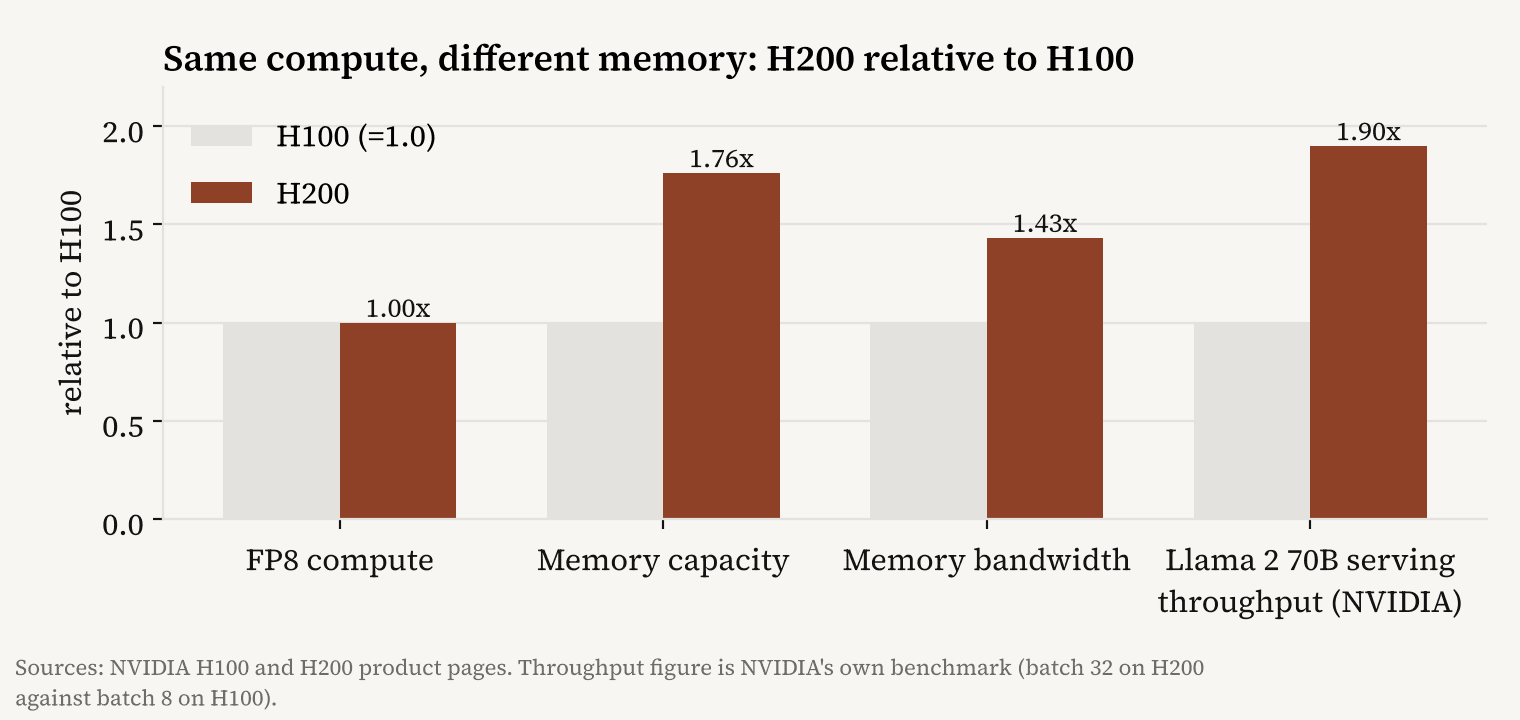
A part with zero additional compute delivered nearly double the serving performance, and it rents at a substantial premium. If someone tries to sell you compute on TFLOPS alone, this is the example that shows you know better.
Two lessons sit inside that pair, and the rest of the series rests on them.
Two chips with the same compute can have very different economic value. The spec sheet's headline did not move; the price did.
The same premium can be worth a great deal to one buyer and almost nothing to another. For a buyer fine-tuning small models, the H200 is an H100 at a markup. For a buyer serving a 70B model at long context, it is nearly twice the machine.
Get out of the habit of thinking "an H200 is 1.5 H100s." Get into the habit of asking "what is this buyer waiting on?"
What is inside the thing called a GPU
The module a spec sheet calls a GPU is not a chip. It is an assembly, and each layer of it affects the price differently.
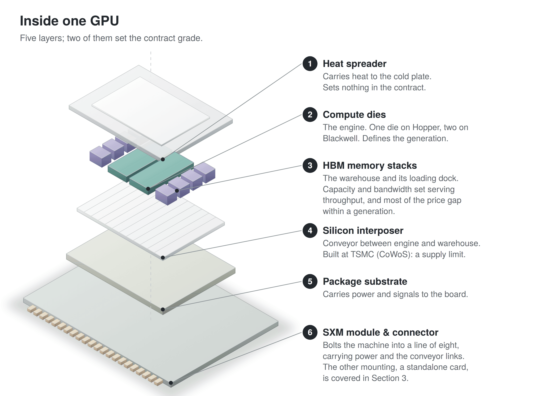
The compute die. The silicon rectangle. On the current generation there are two of them, each close to the largest area a chip-printing machine can expose in one shot, roughly 800 square millimeters.8 NVIDIA's previous generation used a single 814 mm² die with nowhere left to grow, so the next one went to two, joined by a 10 TB/s link fast enough that software sees one GPU. That is why a new generation is a different product rather than a bigger one.9
The HBM stacks. Six or eight towers of memory dies sit beside the compute die, each stack wired vertically through microscopic conductors drilled through every layer. That construction is where HBM's bandwidth comes from, and it is why HBM is expensive and supply-constrained. For the dominant use of GPUs today, the memory's capacity and bandwidth set throughput while the compute die mostly waits. When a new generation commands a premium, much of the premium is for the memory.
The interposer and package. Die and memory sit on a slab of silicon used purely as ultra- dense wiring, because an ordinary circuit board cannot carry thousands of connections at that pitch. The process that bonds die, interposer and HBM together is called CoWoS, and it is done at TSMC. Packaging capacity, not chip fabrication, has repeatedly been the binding constraint on how many accelerators exist in a year.10
The mounting. The package sits on a module that bolts into a baseboard with seven others, delivering 700 to 1,400 W of power and carrying the NVLink connections out to the switch chips that join the eight. The same package on a PCIe card, the kind that slots into an ordinary server, has none of that, which is why PCIe parts cannot join an NVLink domain and why they trade at a discount. Part 3 covers this.
The node. Eight modules on one baseboard, four or six switch chips joining them, two host CPUs that orchestrate but do almost none of the arithmetic, eight network cards at the rear that are the only exit to other nodes, and the power supplies and cooling that keep it all alive. NVIDIA's own 8-GPU H100 server is rated at about 10.2 kW.11
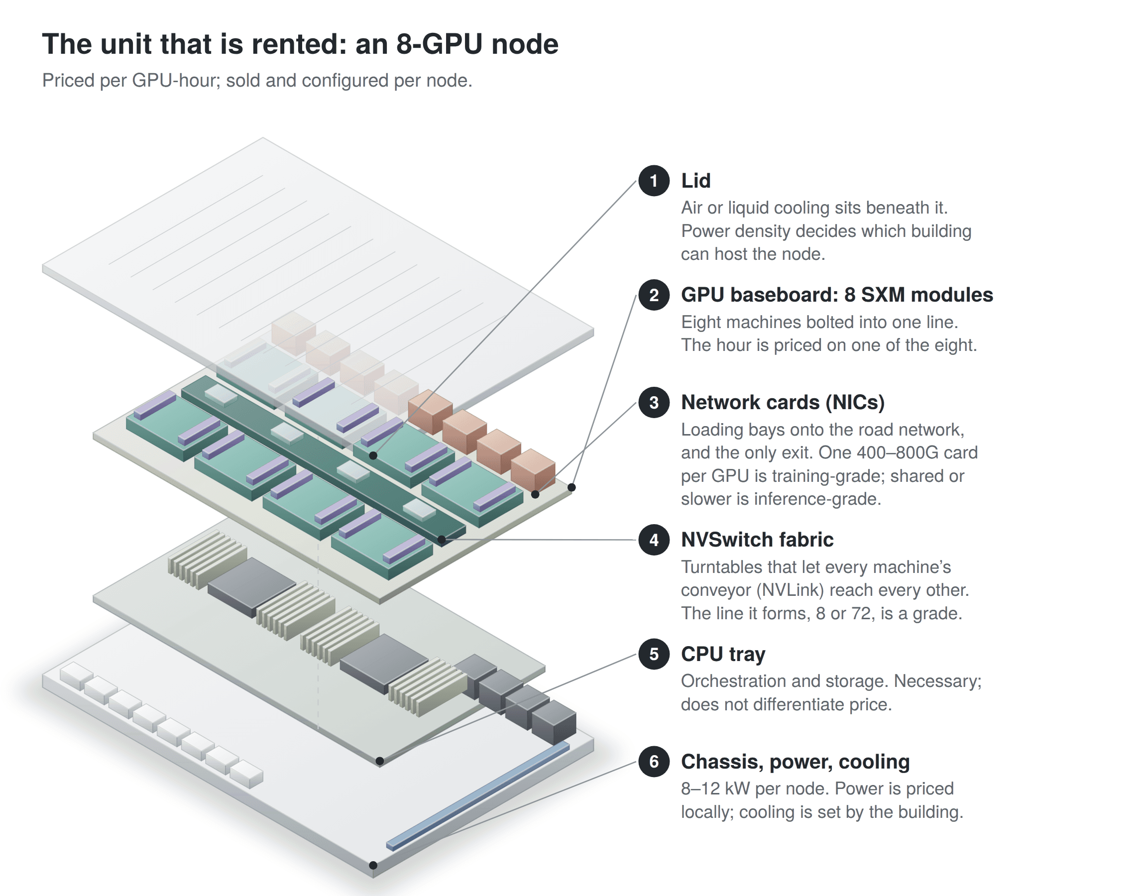
The rack and the cluster. Conventional racks hold four such nodes under a shared network switch, 30 to 40 kW, cooled with air. NVL72 racks are a different animal: 18 compute trays and 9 switch trays joined by a copper spine so that all 72 GPUs share one fast domain, drawing roughly 120 kW, and cooled with liquid because nothing else will do.4,5 Above the racks sit the larger switches that join those together, and the storage that holds datasets and checkpoints, the periodic saves of a training run's progress.
The line that matters most on that tour is the one between inside and outside the fast domain. Inside a node or an NVL72, GPUs exchange data at NVLink speed. Across the network, roughly a tenth of that. Every decision about how to split a model across hardware is a decision about which side of that line the traffic lands on.
Who actually makes a GPU-hour
A GPU is to compute what a turbine is to electricity. Owning the machine does not mean you have a deliverable commodity. You still need the system around it. A GPU-hour is the last link in a chain of nine, and knowing who controls each link is what lets you tell which constraint is binding when someone says supply is tight.
| Link | Who | What they control |
|---|---|---|
| 1. Design | NVIDIA, AMD; captive designers at Google, Amazon, Meta, Microsoft, OpenAI | The architecture. None of them owns a factory. |
| 2. Foundry | TSMC, effectively alone at the leading edge | Fabrication of the compute die. Every leading AI chip is made in Taiwan. |
| 3. Lithography | ASML, sole source | The EUV machines without which leading-edge chips cannot be printed.12 |
| 4. HBM | SK hynix, Samsung, Micron | The memory stacks that drive serving performance. |
| 5. Advanced packaging | TSMC's CoWoS | Assembly of die, interposer and HBM. Frequently the binding constraint.10 |
| 6. Systems | Foxconn, Quanta, Wistron, Supermicro, Dell | The server and the rack, the physical unit that is actually rented. |
| 7. Networking | NVIDIA (Mellanox), Broadcom, Arista, Cisco | The fabric between nodes. |
| 8. Facility | Site developers, utilities, transformer and cooling suppliers | Power feed to transformer to rack to coolant loop. A separate supply chain with multi-year lead times. |
| 9. Capacity owner | Hyperscalers; neoclouds, the GPU-only rental providers such as CoreWeave and Lambda; enterprise clusters | The energized, cooled, networked node. This is who sells the GPU-hour. |
Count the single points of failure in the first five links: one foundry, one lithography supplier, one packaging process, three memory vendors. The physical foundations of this industry are far narrower than its market capitalization suggests. And notice that links six through nine are where a chip becomes a GPU-hour. Someone who thinks only about the first five is thinking about a chip. Someone who thinks about all nine is thinking about the commodity.
[DISCLOSURE]
Published by Rheostat for informational purposes only. Generative AI tools were used in the preparation of this paper. All final content, arguments, and data have been reviewed and edited by the author. This paper is not an offer, solicitation, or recommendation to transact, and is not investment, legal, tax or accounting advice. Market data is drawn from public sources including issuer filings and press releases.
[REFERENCES]
Sources
1 BitOoda, Trading Compute Like a Commodity: What Natural Gas, Electricity, and Agricultural Markets Suggest About Where GPU Compute Trading Is Headed, September 2026.
2 CME Group, "CME Group and Silicon Data to Launch Compute Futures on October 5 to Unlock New Way to Hedge AI Risks," press release, August 11, 2026, and the Compute Futures product page (730 GPU-hours per contract, separate H100 and B200 contracts). The launch remains subject to CFTC review as of early November 2026.
3 Intercontinental Exchange, "ICE and Ornn to Launch GPU Compute Futures Contracts," press release, May 19, 2026.
4 NVIDIA, GB200 NVL72 product page: 72 Blackwell GPUs, 36 Grace CPUs, 13.4 TB HBM3e, 130 TB/s NVLink, liquid-cooled.
5 NVIDIA, DGX GB200 Rack Scale Systems User Guide, Hardware: 18 compute trays, 9 NVLink switch trays, rack power approximately 120 kW; and NVIDIA Technical Blog, "NVIDIA Contributes GB200 NVL72 Designs to OCP," October 2024, on the 120 kW cooling requirement and direct liquid cooling.
6 NVIDIA, H100 Tensor Core GPU product page: 80 GB HBM3, 3.35 TB/s, up to 700 W, FP8 3,958 TFLOPS with sparsity (1,979 dense), NVLink 900 GB/s.
7 NVIDIA, H200 Tensor Core GPU product page: 141 GB, 4.8 TB/s, up to 700 W, identical Tensor Core figures to H100, "Llama2 70B inference 1.9X faster" (the footnote compares batch size 8 on H100 with batch size 32 on H200).
8 WikiChip, "Mask": the maximum lithography field size of 26 mm by 33 mm, or 858 mm²; and NVIDIA Technical Blog, "NVIDIA Hopper Architecture In-Depth": H100 die 814 mm², A100 die 826 mm².
9 NVIDIA, "NVIDIA Blackwell Platform Arrives to Power a New Era of Computing," press release, March 2024: 208 billion transistors, two reticle-limit dies, 10 TB/s chip-to-chip link.
10 The Register, "TSMC CEO predicts AI chip shortage through 2025," July 18, 2024, quoting C.C. Wei that CoWoS packaging capacity "was still the bottleneck" despite more than doubling year on year.
11 NVIDIA, DGX H100 datasheet: 8 H100 GPUs, 4 NVSwitches, about 10.2 kW.
12 Reuters, "ASML plots future of chipmaking tools for AI beyond EUV," March 2, 2026: ASML is the only maker of EUV lithography equipment.
[ABOUT]
About the author
Dev Udata has 6 years of experience in digital assets, quantitative trading, and emerging derivatives markets. His work focuses on prediction markets, compute derivatives, and developing pricing, hedging, and execution infrastructure for emerging asset classes. He holds degrees in Finance and Data Science from the University of Illinois and has passed the Series 3, 7, and 63 exams and completed the NFA Swap AP requirements.